
Explore the benefits of implementing a professional SPI inspection today
In April 2022, we installed a new solder paste inspection (SPI) device on our SMT shop floor. The installation of the SPI was preceded by a multi-hour selection process, part of which involved ongoing tests of equipment from various manufacturers.

Why is the use of SPI (Solder Paste Inspection) of great and growing importance to customers of EMS service providers? The simple explanation that it is about quality is not enough, as there is a quality objective in the background of almost every investment in machinery.
The last two years have been a particularly difficult time for electronics manufacturers. The confluence of natural catastrophes and the COVID-19 pandemic, the breakdown of supply chains and even political tensions and armed conflicts have not favoured electronics manufacturers, who are experiencing shortages in the availability of electronic components.
Customers cannot afford the risk of faulty PCBAs, as components wasted in a faulty assembly process may not be available for months. In a situation where up to 60% of defects in SMD assembly can be attributed to the paste printing process, the quality dimension of investment in SPI is paramount.
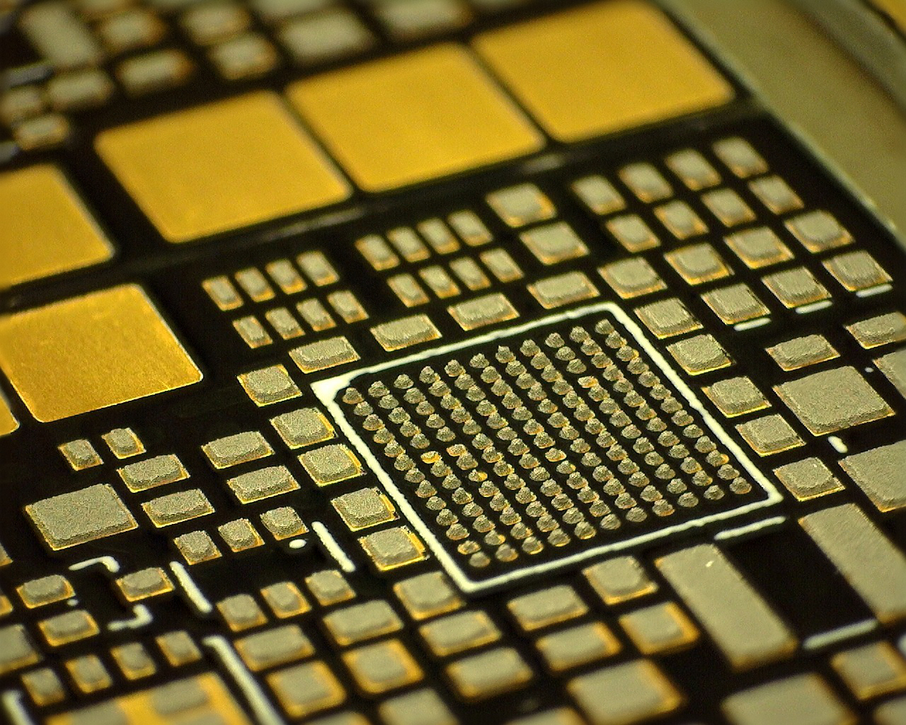
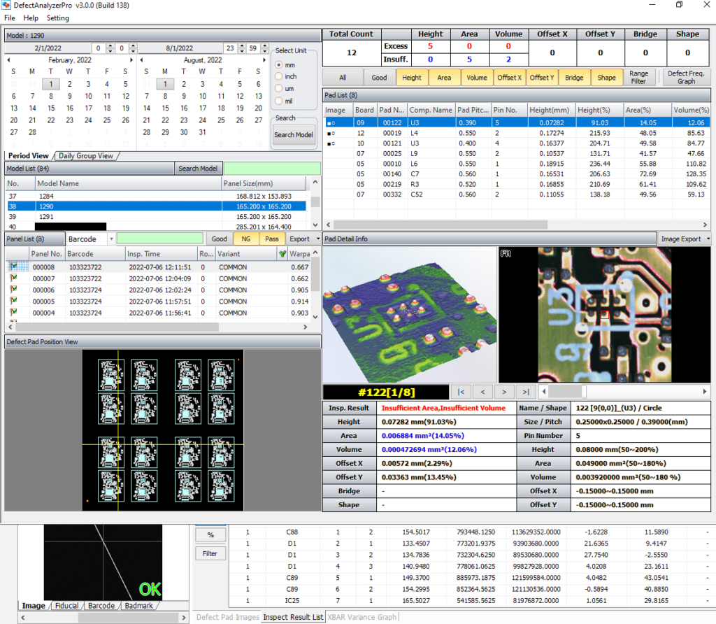
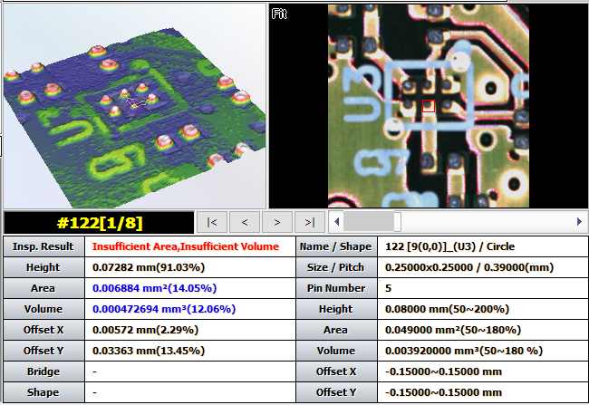
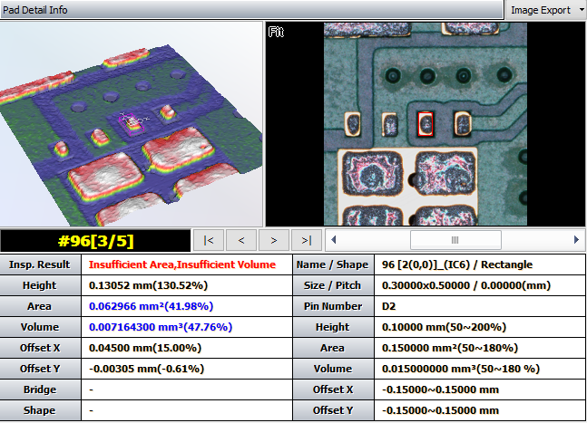
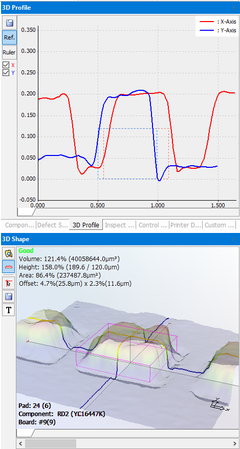
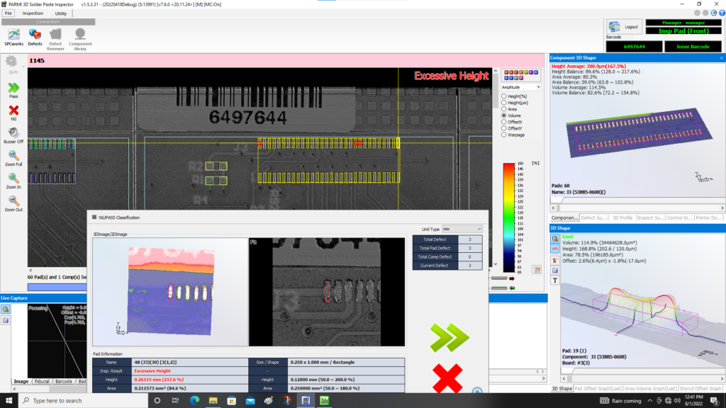
Solder Paste Inspection devices support the process of solder paste being applied by the printer on the PCB. SPI can accurately measure paste volume, offset, pad coverage area, detect bridging and check special conditions such as deposit deformation or paste volume differences on individual pads of a single component. Thanks to very fast algorithms, 100% of the board surface is analysed without affecting assembly line performance. Full information on each paste deposit is fed into the SPC Data statistical module, ready for further analysis.
Physically, the SPI is a small device located between the printer and the pick & place machine and preferably it should display PASS throughout its operation. However, in order to be sure that this message is real, that the SPI can be trusted, we undertook a process of precise comparison of the solutions available on the market, while carrying out tests of the manufacturing processes.
The suppliers we shortlisted were even tortured by us with detailed questions, which even ended up reaching the manufacturers’ R&D engineers on several occasions. This is because we do not accept ‘unnecessary options’. We learn the principle of operation in depth, with all the intricacies, so that we can use the full functionality of the instrument and be confident of the results obtained regardless of interference factors. We were determined to such an extent that, as part of our tests, we physically verified paste volume measurements by taking the increase in weight of the board after printing on a precision balance. Do we not trust the suppliers? We trust our own experience, the knowledge that is our advantage!
Ultimately, we chose a device that met our expectations and, after a period of implementation, our customers are already reaping the benefits. We can now see what was not visible before. The figures allow us to better understand the process and adjust it more precisely for each project.
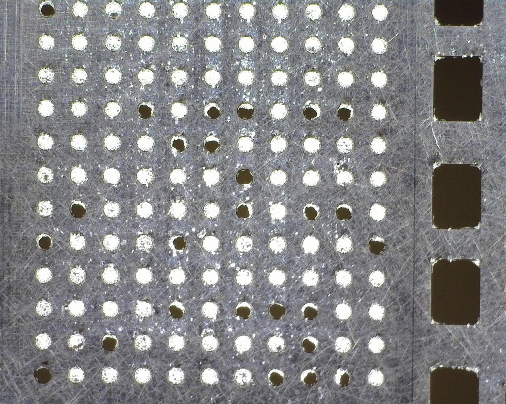
Based on the potential of SPI, our process engineers decided to launch their own R&D project: improvement of the process capability for small aperture paste printing.
As components become smaller and smaller, and stencil apertures become almost invisible to the bare eye, the amount of paste remaining in the stencil after printing increases. The most dangerous defects are hidden ones, resulting, for example, from too little paste on the pad, as then no proper joint is formed and you only get a ‘contact’, a connection that is mechanically unstable. Such defects are detected neither by the standard 2D control built into the printer nor by functional tests of the finished product.
In our research and development project, supported by the SPI, we look broadly at the printing process. We analyse its dependence on factors such as the choice of paste, stencil material and technology, the use of additional nano-coatings or the influence of design aspects on the final result. We collect and analyse the data in the SPC module.
The findings of our proprietary research are intended to help us select the best solutions in the process of assembling highly complex PCBAs, since we see this as a benefit to our customers.
It is easier to avoid problems than to eliminate them, which is at the centre of our philosophy and entitles us to take on an advisory role for our customers.
Among the interesting facts worth mentioning is the colour of the PCB. If our customer prefers PCBs in a colour other than green, we have good news – our machine provides unwavering accuracy on any soldermask colour, which we thoroughly checked before purchase and which is not at all as obvious as claimed by most SPI manufacturers.
Our engineers will be happy to provide you with further information. Please feel free to contact us by email at ems[at]jm.pl