
How to avoid the most common PCB design mistakes? Practical tips for better PCB design
Printed circuit board (PCB) design is a critical stage in developing electronic devices. It affects not only the reliability of the circuit but also production costs, ease of assembly, and maintainability. Even minor design errors can lead to costly rework, production downtime, or quality issues in the final product, particularly for companies in the Electronics Manufacturing Services (EMS) sector.
In this article, we highlight the most common PCB design mistakes and provide practical guidance on how to avoid them.
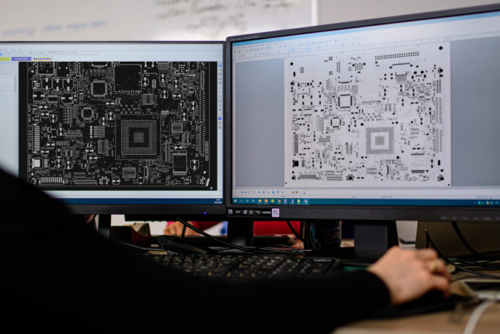
Production documentation is essential for communication between the designer and the EMS partner. Missing files – such as Gerber files, the BOM, pick-and-place files, or assembly drawings – or inconsistent labeling, such as mismatched item numbers between the schematic and the PCB, can slow down assembly preparation, causing delays and additional costs.
Using standardized documentation practices, thoroughly checking file consistency, and generating documentation directly from CAD software (e.g., Altium, KiCad) can prevent errors. Including a PDF view of the board, a layer diagram, and a component table further ensures clarity.
The BOM is crucial for component procurement. Missing manufacturer part numbers, tolerance values, or package types can result in incorrect orders, production delays, and discrepancies between prototypes and final products.
Maintaining a detailed and up-to-date BOM that includes reference designators, component names, values, tolerances, packages, manufacturer part numbers, and possible substitutes is essential. Generating the BOM directly from the CAD system and applying version control helps maintain accuracy.
Sometimes the footprint, meaning the pad layout and dimensions, does not match the actual component. Even small discrepancies, such as different lead spacing, can prevent proper placement, requiring manual adjustments or, in extreme cases, scrapping entire boards.
Using component libraries from trusted sources, such as manufacturers or certified databases, and verifying footprint dimensions against datasheets during the design stage prevents these issues.
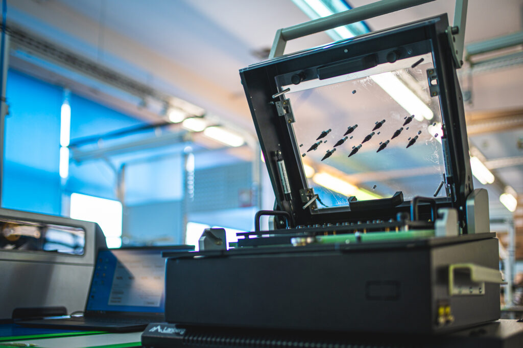
Unclear markings for diodes, electrolytic capacitors, or integrated circuits can lead to orientation errors. Pick-and-place machines require accurate information about pin 1 or component polarity; missing or ambiguous markings increase the risk of incorrect assembly or necessitate additional consultation with the designer.
Including clear assembly drawings and marking components with defined rotation ensures correct placement.
Holes in THT (Through-Hole Technology) pads that are too small can prevent proper pin insertion, and solder may not fill the hole completely, reducing connection quality.
The hole diameter should be at least 0.2–0.3 mm larger than the lead, and PCB manufacturer specifications for minimum drilling tolerances must be observed. Creating a test panel to measure actual hole dimensions after metallization is recommended.

If a design does not meet the minimum spacing requirements specified by the manufacturer, such as 6 mils for both track width and spacing, short circuits may occur, and production costs may increase significantly. In extreme cases, the board may require an HDI process, which substantially raises manufacturing costs.
Setting DRC (Design Rule Check) rules according to the manufacturer’s parameters from the start of the design and using CAD tools to detect violations ensures compliance before exporting Gerber files.
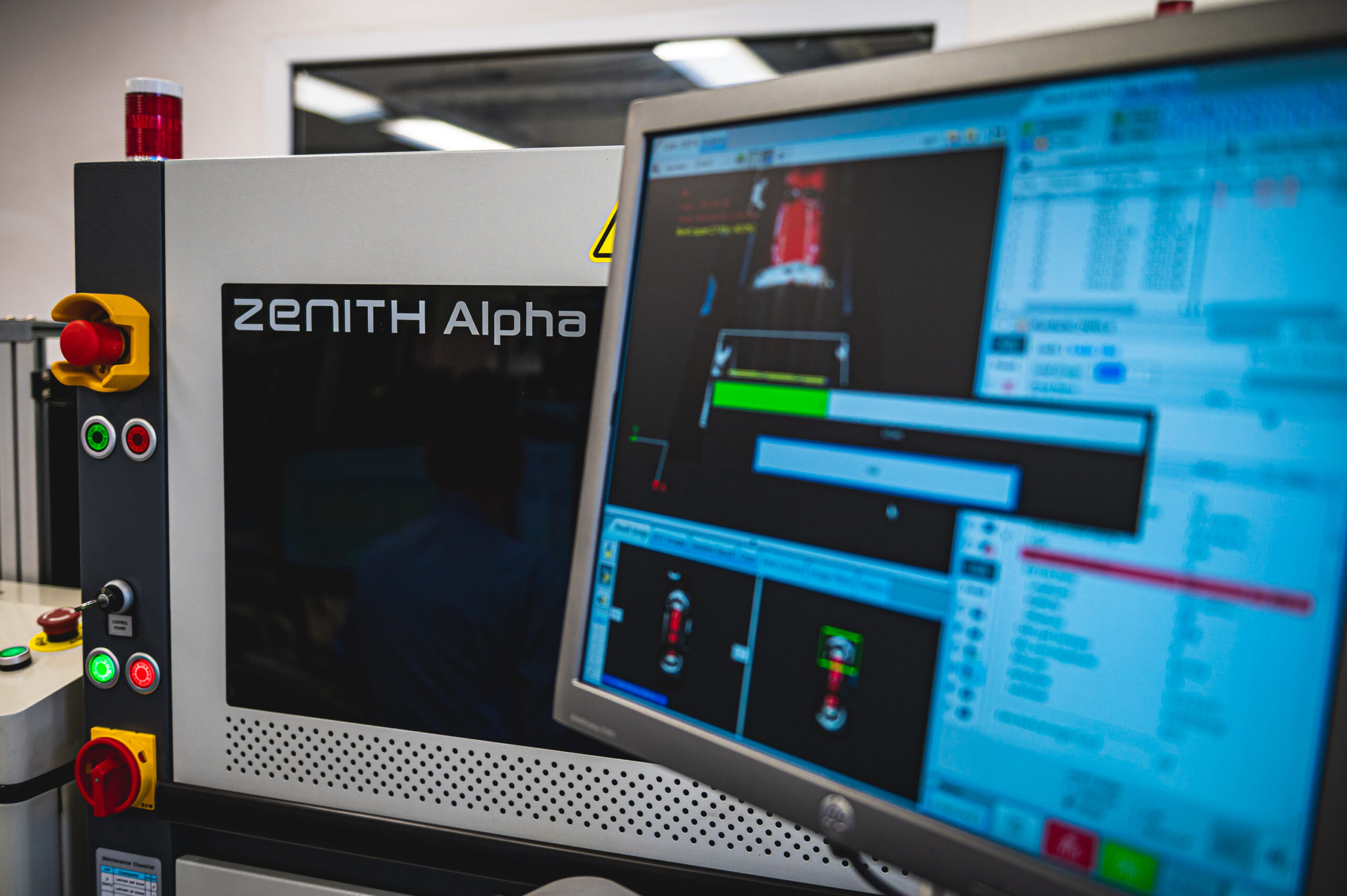
Fiducials are essential markers that allow pick-and-place machines and automated optical inspection (AOI) systems to determine board orientation. Without them, the EMS partner may need to add fiducials manually or adjust the design, leading to delays and additional costs.
Panelization is usually performed by the EMS partner according to their process requirements, including adding a frame (typically 5–10 mm wide) and at least three fiducials in the corners of each module.
Test points are crucial for quality control and functional testing, including ICT (In-Circuit Testing) and FCT (Functional Circuit Testing). Their absence complicates diagnostics, prolongs testing and servicing, and sometimes necessitates temporary wire soldering, which increases costs.
Including test points for critical signals, power supply lines, and ground connections at the design stage ensures easy access for test probes, ideally with a minimum diameter of 1 mm. Some CAD tools can generate these points automatically.
Components placed too close to each other or near the edge of the board may interfere with pick-and-place nozzles, soldering tools, or the enclosure. Insufficient spacing also complicates rework and inspection. Placing components less than 3 mm from the board edge increases the risk of damage during depanelization.
Maintaining minimum distances between SMD components and leaving 3–5 mm from the board edge, along with performing 3D CAD analysis, helps prevent interference with the enclosure and assembly tools.
Choosing unusual laminate thicknesses, such as 0.9 mm, or suboptimal stack-ups can create assembly difficulties and increase production costs.
Consulting the PCB manufacturer during the design stage and using standard stack-ups, such as a 4-layer FR4 configuration, ensures manufacturability. If a specific stack-up is required, verifying its availability and including the specifications in the PCB documentation is recommended.
If component markings or values overlap pads, soldering may be hindered and solder paste contamination may occur. Conversely, missing markings complicate service and troubleshooting.
Checking silkscreen placement using CAD tools and maintaining a minimum distance from pads, typically 0.2 mm, ensures readability. Using clear fonts and avoiding overly small markings improves overall legibility.
Insufficient space between SMD pads can prevent proper application of the solder mask, resulting in solder bridges during assembly and potential short circuits.
Using manufacturer-recommended footprints, applying solder mask expansion in CAD tools, and verifying compliance through DRC checks prevent these issues and reduce manual rework.
PCB design requires precision, experience, and thorough knowledge of manufacturing standards. Even small errors in documentation, footprints, or component placement can significantly impact both cost and reliability. Close collaboration between the designer and the EMS partner, adherence to DRC rules, verification of data consistency, and early consideration of assembly and testing requirements are key to successful production.
Conscious and careful design not only prevents costly corrections but also ensures quality, stability, and professionalism throughout the manufacturing process. At JM Elektronik, we assist with comprehensive design verification, documentation optimization, and board preparation for efficient assembly.
Reduce the risk of errors by designing your PCB in collaboration with EMS experts.